

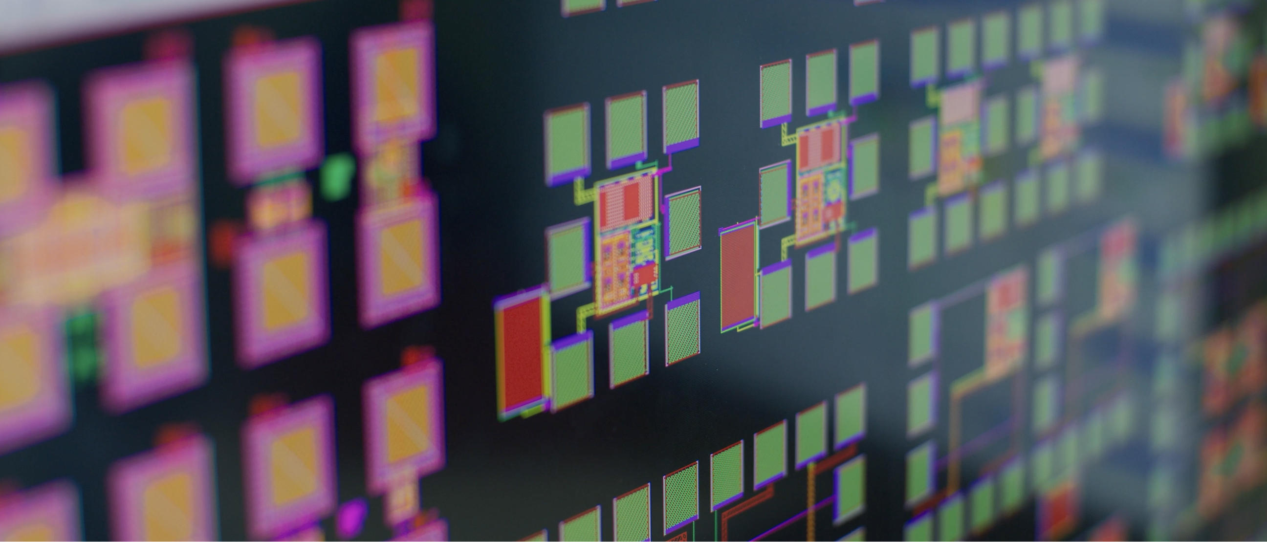
The process development kit (PDK) serves as a crucial bridge between the design of an integrated circuit and semiconductor foundries for chip fabrication. Staera offers unique and comprehensive solutions to support large-scale circuit simulation, design and layout verification through its integrated CMOS + GaN PDK (iPDK). This iPDK enables the design and fabrication of circuits on Staera’s proprietary integrated CMOS + GaN wafer technology.
The iPDK libraries are tailored to Staera’s CMOS + GaN offerings, making them ideal for unique applications that go beyond the offerings of conventional CMOS or GaN foundries. To achieve a robust and reliable bridge between integrated circuit design and fabrication, the process development and IC design teams at Staera have worked closely together, fine-tuning every aspect with meticulous attention to detail, thereby enabling a new age of integrated circuit design. This ensures that the challenges of III-V/Si integrated circuit design and fabrication are overcome, ushering a new paradigm of chip-based solutions for optoelectronic systems such as optical interposers.
If you would like to learn more about our circuit design process or how Staera chip solutions can support your applications, contact us at contact@staera.ai.
%201.jpg)