

Compound semiconductors do the things silicon cannot do. Emit light. Control high power. Transmit ultra-high frequency. Amplify the most challenging signals. Compound semiconductor components are assembled with silicon chips in the devices that help us see, connect, and move.
But the promise of compound semiconductors is only partly met, because they don’t integrate and scale like a silicon integrated circuit.
Staera fully integrates compound semiconductors into silicon chips. Realization of the full potential relies as much on integrated design as it does on integrated materials. The whole turns out to be greater than the sum of its parts.
Designing a CMOS chip for leading edge performance requires the integrated design environment that evolved in integrated silicon CMOS manufacturing. These chips hold millions to billions of devices, all switching and regulating in concert, and a designer must be able to connect and control them all to deliver leading-edge capability. That is why chips are designed in electronic design automation (EDA) software. Consider EDA software an earlier form of software intelligence. The software aids the designer in figuring out how to place and interconnect millions or billions of transistors so that the final chip works according to plan.
A single silicon process involves hundreds of manufacturing steps and patterns to produce the plethora of silicon devices, so an enormous amount of information passes between the foundry that fabricates a chip and the designer who creates it. The EDA software embeds that information in a “PDK”.
A PDK gives the designer and foundry two assurances: that a submitted design is manufacturable, and that the circuit will work as intended.
Foundries supply design rules, such as how close two devices may sit and how wide the metal traces between them must be. Each transistor, each device comes as a parameterized cell (P-Cell) with a schematic symbol, a physical layout and a device model describing its electrical behavior in simulation. The PDK also captures the range of manufacturing variation, from slow devices to fast ones, so designers can confirm a circuit works anywhere within the manufacturing variance.
PDKs also carry design acceleration and verification tools. As designs have increased the number of transistors and other devices, those have become critical to holding down cycle time and designer headcount.
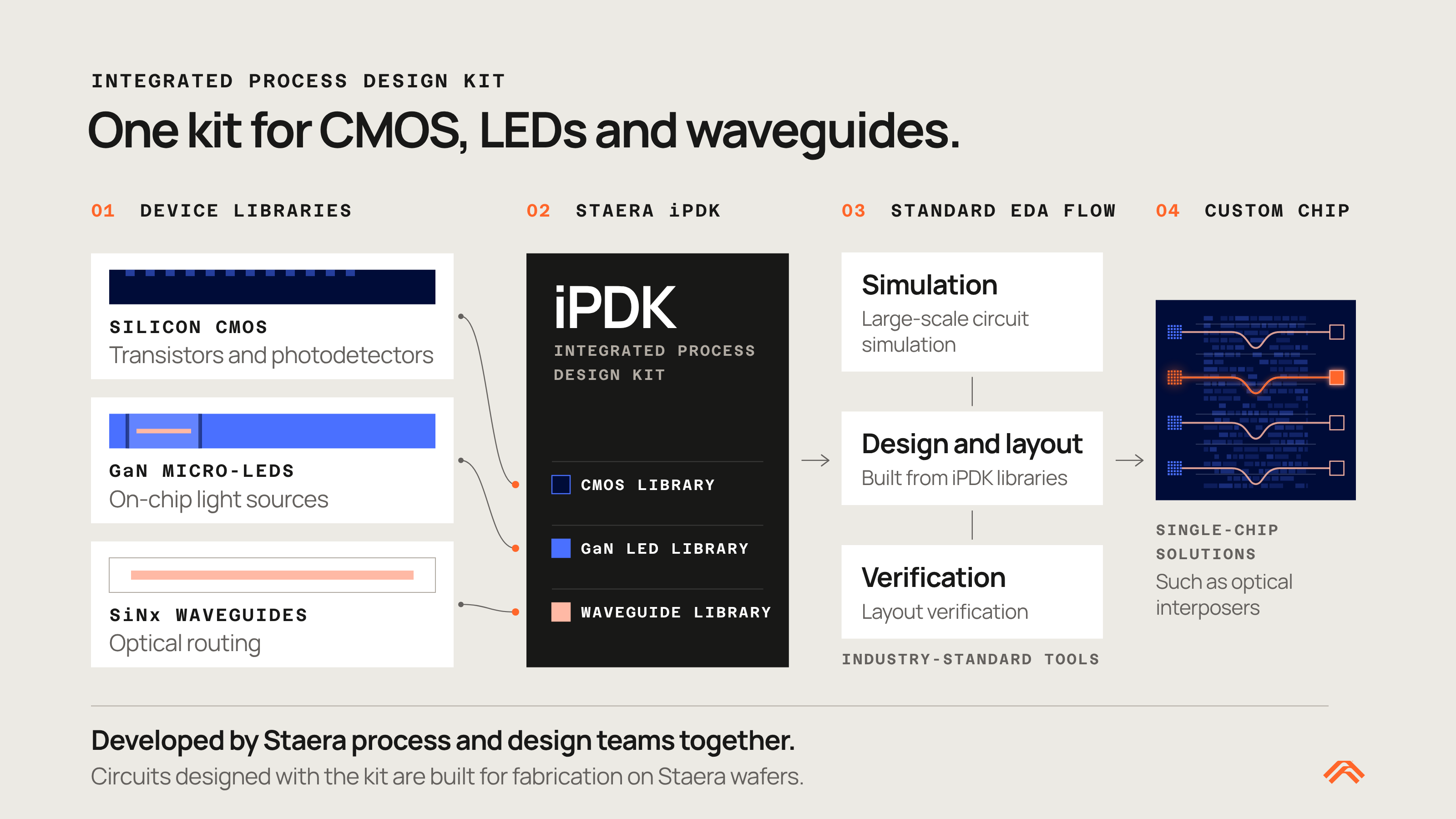
A foundry CMOS PDK has everything needed to design a CMOS chip. Staera's process puts two more technologies into that chip: GaN LEDs for generating light, and waveguides for optical signal routing.
So, we built an integrated PDK, extending commercial silicon PDKs with GaN LEDs and waveguides that lets our team design, simulate, lay out and verify all three in one automated flow. We add proprietary LED P-Cells, waveguide layers, design rule files and simulation tools to the foundry’s CMOS PDK. LEDs do not behave electrically like CMOS devices, so they need their own models; we use a mix of proprietary and open-source models to predict their electrical and optical behavior.
The result is a flow where a designer familiar with CMOS circuit design can incorporate LEDs and waveguides into their circuits without needing to learn anything new in their EDA software and build chips that do things neither CMOS nor LEDs can do alone.
Design certainty. One of the hardest problems in combining CMOS and LEDs on separate chiplets is proving that a chiplet from one unknown process corner will work with a chiplet from another. Driving LEDs takes precise analog signals, specific bias voltages and currents rather than digital ones and zeros, so the design is especially sensitive to process drift. When CMOS and GaN devices are built on the same wafer, they share equipment, facilities and thermal treatments, so their process corners are partly correlated. A circuit that passes across all simulated corners is far more likely to meet specification in silicon.
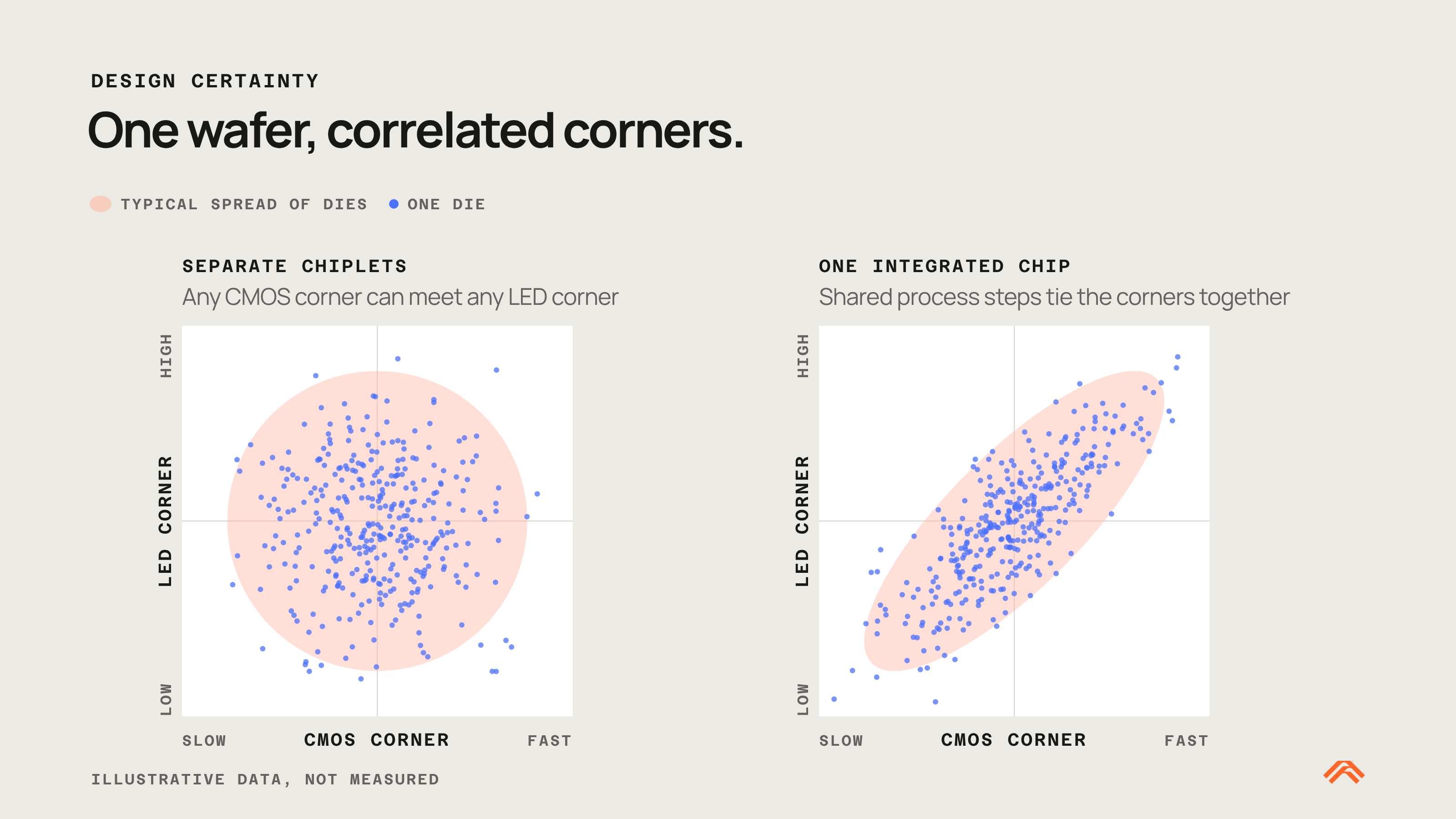
Performance. Pushing a technology to its limits means optimizing safety margin, and greater confidence in simulation is what lets us be more aggressive in reducing it. Discrete chiplets have to carry larger margins, which costs both performance and yield.
Application-specific tools. Lightwire combines GaN LEDs, silicon nitride waveguides and CMOS circuits including photodetectors, so its design tools must understand light as well as electrical current. Our design infrastructure integrates with industry-standard tools and plugins, and we bring simulation of optical propagation, loss and crosstalk into the circuit design environment. That unifies what is otherwise two separate efforts, photonic and electronic.
Cycle time. Designing several chiplets takes longer than designing one chip, because each carries its own overhead. Design rule checks and layout-versus-schematic checks have to run on every chiplet, and then the chiplets must be verified against each other. A single integrated chip runs that gauntlet once. The result – shorter design cycles, and lower upfront engineering costs.
Together, these advantages let us build chips that no single-technology process could produce, for customers across several fast-growing applications.